PCB files for board manufacture |
Component overlay |
Component list |
Circuit schematic |
Design files |
PCB plots |
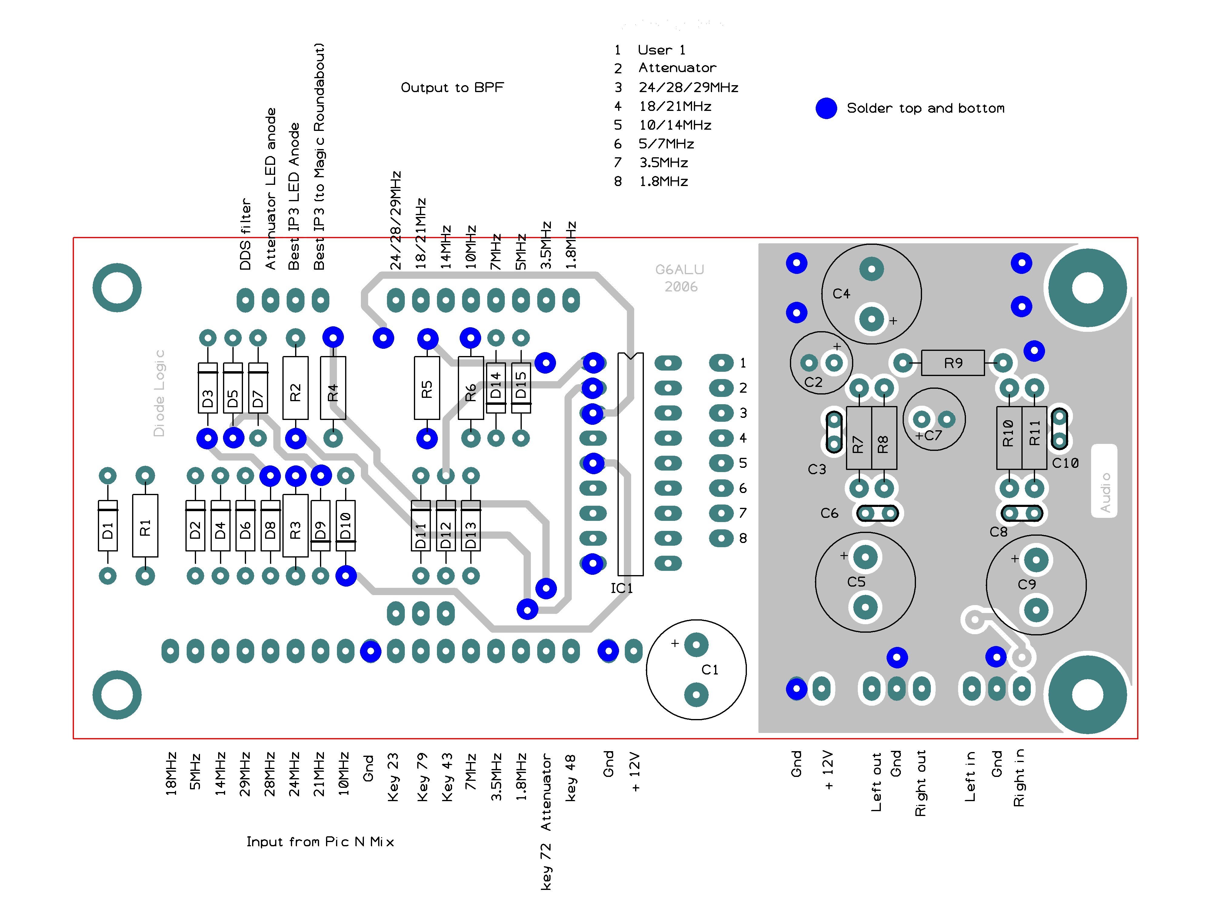
PCB Overlay |
Component list |
Circuit schematic |
Not currently available |
PCB dimensions - 108 x 50.9mm to the outer edge of PCB outline
Date |
Item affected |
Change |
| 06-01-07 | PCB Overlay | Labels "user 1 and Attenuator" swapped |
| Added construction notes | ||
| 13-02-07 | PCB Overlay | Labels "Best IP3 (to magic roundabout) and best IPs LED anode swapped |